
Ultra-efficient RF components, Made in the USA
Falcomm's patented Dual-Drive architecture drives the gate and source of a power amplifier simultaneously. The architecture spans CMOS, SOI, GaN, and GaAs and supports catalog parts and custom silicon for satellite, telecom, and defense systems.
K-band efficiency, ready to ship.
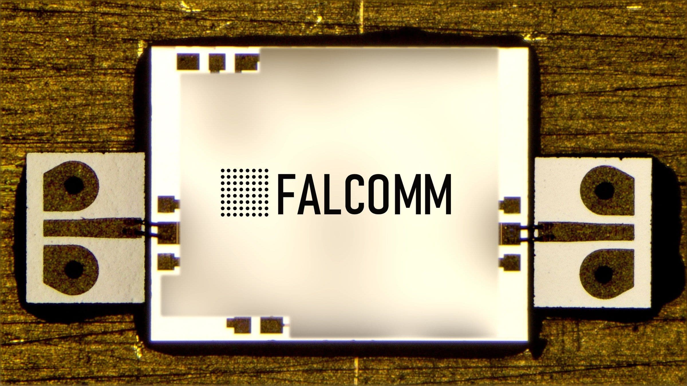
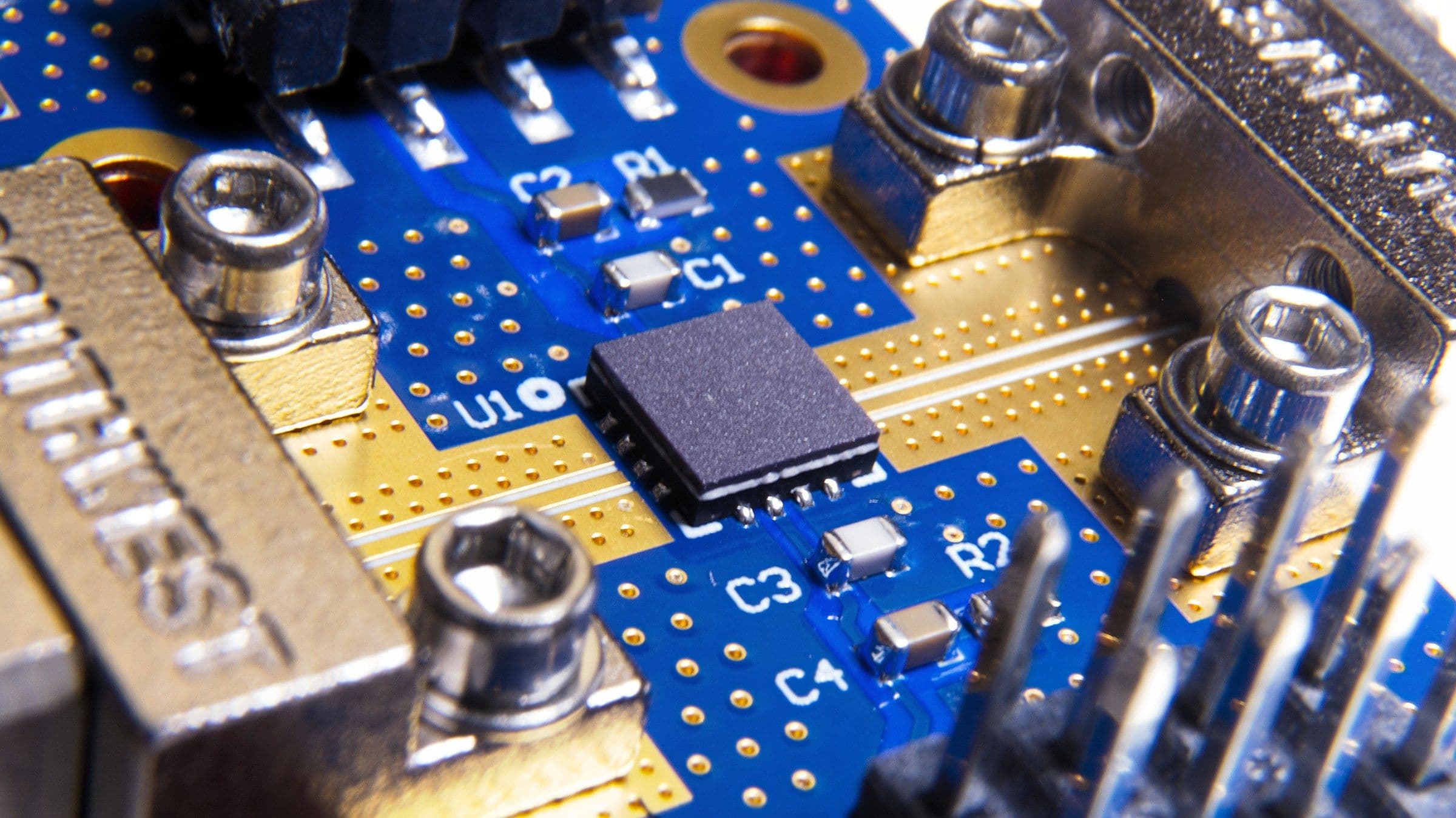
K-band GaN power amplifier for SATCOM and defense terminals. 44% PAE at 36 dBm Psat, available packaged or as bare die.
The Falcomm Advantage.
Next-generation wireless systems are increasingly data-intensive and performance-driven. Falcomm's patented Dual-Drive™ Power Amplifier technology delivers more output power, wider bandwidth, and less heat for mission-critical applications.
Space
- Reduce battery consumption
- Reduce thermal management costs
- Reduce launch costs
Telecom
- Increase range
- Reduce carbon footprint
- Decrease energy cost
Defense
- Increase power
- Reduce thermal management costs
- Reduce size & weight
Custom Design
- Best in class efficiency
- More RF power
- Less heat
From Atlanta to orbit.
Designed and manufactured in the USA. Validated in CMOS and GaN.
More RF power, less heat.
The power amplifier sets the ceiling for everything else in an RF system. Falcomm's patented Dual-Drive™ architecture drives the transistor's gate and source simultaneously, lowering its effective knee voltage so more of the DC supply comes out as RF power instead of heat.
IEEE ISSCC 2021 reported a measured result of 50% peak PAE and 60% drain efficiency at 30 GHz.
The same DC budget pushes more signal out of the antenna.
Smaller heat sinks, simpler thermal design, and less mass to launch.
Falcomm's published design flow models within 2% of measured results.
Validated across the processes Falcomm supports.
Advanced nodes for integrated mmWave front ends.
45RFSOI and FD-SOI nodes for efficient mmWave integration.
Watt-class output for C, Ku, and K-band systems.
Proven RF performance where the system demands it.
Measured results, published research, and patents.
The foundational Dual-Drive paper reports measured silicon results. Related IEEE research and issued patents show the broader technical work behind Falcomm.
These issued U.S. patents are listed in Falcomm's June 2026 company brochure.
One lab, DC to 150 GHz.
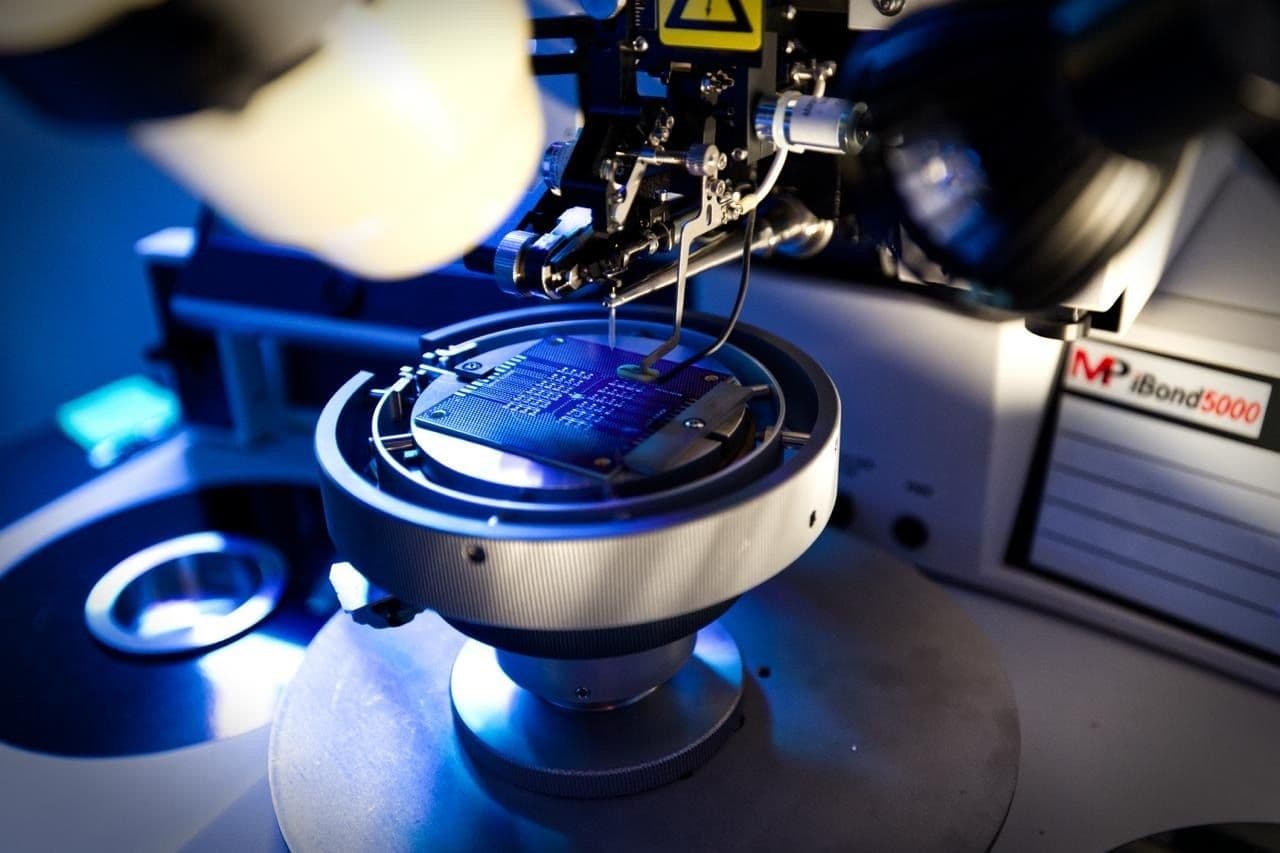
Falcomm's in-house RF and mmWave lab measures parts from DC to 150 GHz: continuous-wave, small-signal, modulation, and VSWR testing under one roof. Design and measurement sit in the same Midtown Atlanta office, so a part moves from model to silicon to bench data without leaving the building.
GaNdalph.ai
GaNdalph.ai is Falcomm's AI-native EDA software for power amplifier design, trained on process data developed alongside GlobalFoundries. It reduces a months-long design cycle to minutes for single- and two-stage RF PAs on GF RFGaN1.
Describe the spec
Give GaNdalph the same brief you'd hand a design team: frequency, output power, efficiency, and process node.
Search the design space
Falcomm's foundation models explore metal-stack EM physics, transistor nonlinearities, and manufacturability rules.
Generate the design
GaNdalph produces a layout-ready design against the rules of a qualified GlobalFoundries process.
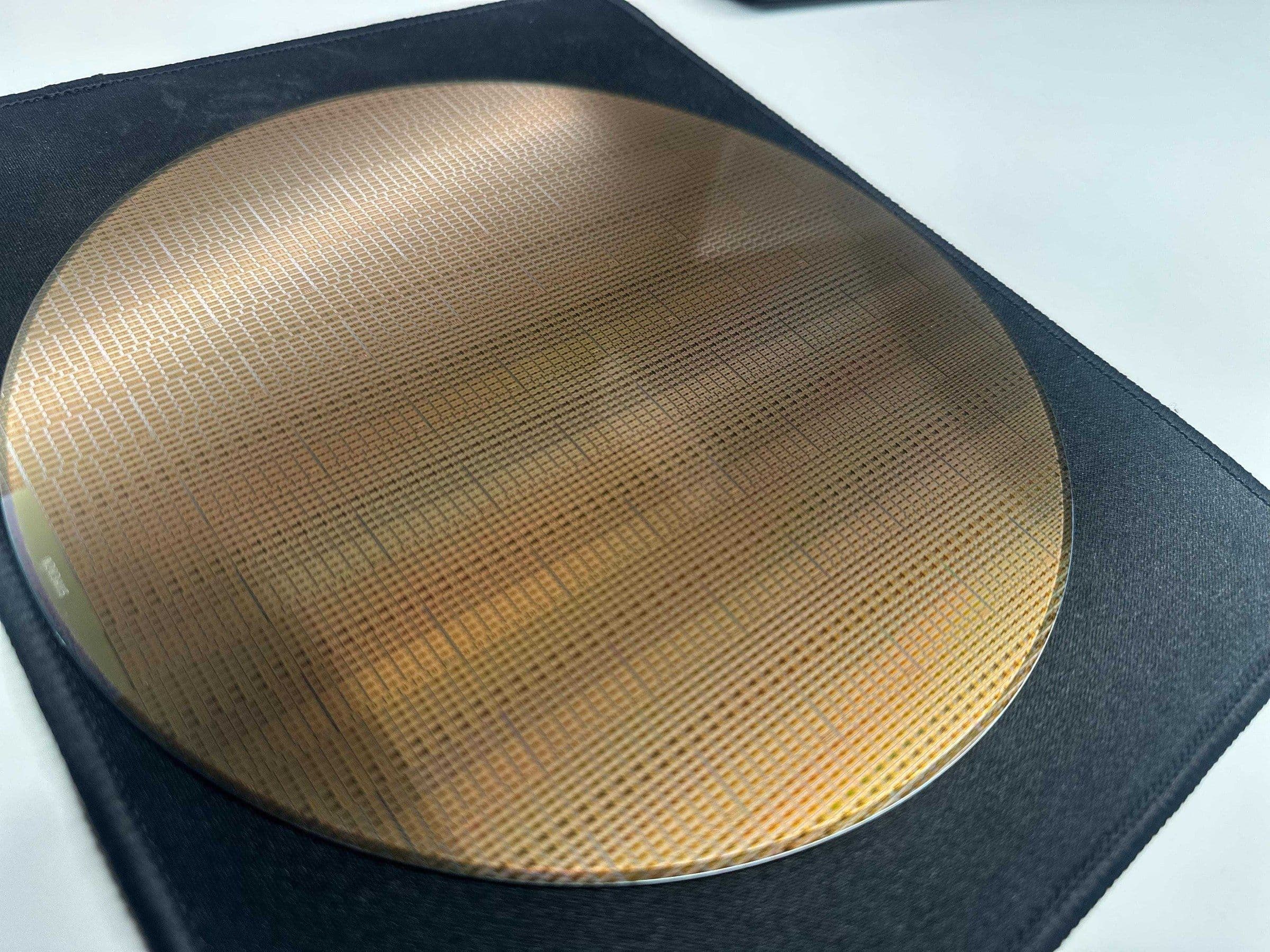
Priority access to advanced CMOS, GaN, SiGe, and GaAs process nodes, backed by a strategic partnership with GlobalFoundries.
Built on U.S. partnerships, Falcomm delivers reliable, homegrown semiconductor solutions with full supply chain transparency.
From prototype assembly and test through high-volume OSAT, Falcomm supports parts from first articles to production.